The RS Flip-Flop
This is the
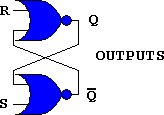
Set-Reset Flip Flop logic block. Although it is called RS, it is said
to stands for Set-Reset*. You can see that the inputs of one NOR GATE
receive from the output of another. Note the point where the two wires
cross (make an X). This is not a point of connection. It could,
alternatively, be drawn like this:
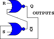 In this form the wires do not
cross and it is clear that there is no direct connect between the two
outputs. However, in more complex circuits it is sometimes not possible
to find an "alternative" path and the lines have to cross. The
rules for connections are illustrated below.

The special
ability of an RS Flip Flop is to "remember" the last state it was set
in. NEW TERM: SET means changed to the value of 1 and RESET means
changed to 0. In otherwords, the RS flip flop is a 1 bit memory. It can
retain the state of either a 1 or a 0. A bit is like a digit, only it
is for binary. We use the decimal number system, also known as base 10.
We have 10 numbers {0,1,2,3,4,5,6,7,8,9}. In binary there are only two
numbers to use {0,1} A single "digit" in binary is called a bit. You
may have heard the term byte before or mega byte. One byte is equal to
8 bits and a MB is equal to about a million bytes. With a little
modification 8 RS Flip Flops could be used to make a 1 byte memory!
An example of a bit ( 0 )
An example of a byte ( 01010101 )
To learn more about the binary number system CLICK HERE
Lets assume that the R and S values for the RS flip flop are both 0. What would the Q and be? Lets try
to use the skills from the previous lesson to figure it out...
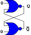
It seems like there is some information missing. We can't determine the output of either gate since the gates take inputs from the outputs!!
However, we could try using the truth table of the NOR GATE as a guide, we know that if 1 or both of the inputs is a 1 then the output has to be 0. But, since the value given for R and S is 0 we can't mathematically determine the result of either gate. It could be 1 or 0. Electronically, though, what would happen...? Because of slight imperfections in the transistors themsevles along with electrical characteristic variations in the wires that connect them one gate will turn on slightly faster than the other, maybe only by nanoseconds.

Lets say gate 1 turns on first. Since gate 2 is still off, it has an output of 0. Gate 1 takes the output value of 0. Since Gate 1 has two 0's for outputs, it's output becomes 1, based on its truth table. Meanwhile... gate two powers up. It takes the output from gate 1 (1) and its output becomes 0, which it was when it was "off". The loop stops and the circuit stabilizes. This is called a stable state. It will remain in this state unless there is a loss of power or S/R are changed.
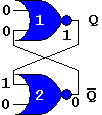 Circuit
stabilized...
Every time you power up this circuit it could initialize in a different state, because of electrical variations. Q will always be the opposite of or vice versa, however. When doing
these circuits on paper, you have to "make up" a state it starts in.
After that you can calculate the changes based on the inputs.
Here is the Truth table for the RS Flip Flop. You should be able to derive this from the circuit on paper...
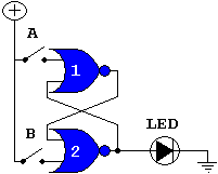
A circuit like this could be built... When switch A is pressed down the LED lights, nothing special yet. When switch A is released, however, the light continues to glow! The R-S Flip Flop "remembered". Now press button B. The LED goes off and if there was an LED attached to the other gate it would now turn on. When button B is released the LED stays on. Once again, the circuit retain it new state. If both buttons are pressed both LEDs would light, but this is a disallowed state because the circuit will not retain the memory of two LEDs on, As soon as the buttons are released, the circuit will return to some unpredictable, but stable, state. If the same button is pressed twice or more in a row, nothing happens.
Click on image above for an interactive simulation
An example of a bit ( 0 )
An example of a byte ( 01010101 )
To learn more about the binary number system CLICK HERE
Lets assume that the R and S values for the RS flip flop are both 0. What would the Q and
 be? Lets try
to use the skills from the previous lesson to figure it out...
be? Lets try
to use the skills from the previous lesson to figure it out...It seems like there is some information missing. We can't determine the output of either gate since the gates take inputs from the outputs!!
However, we could try using the truth table of the NOR GATE as a guide, we know that if 1 or both of the inputs is a 1 then the output has to be 0. But, since the value given for R and S is 0 we can't mathematically determine the result of either gate. It could be 1 or 0. Electronically, though, what would happen...? Because of slight imperfections in the transistors themsevles along with electrical characteristic variations in the wires that connect them one gate will turn on slightly faster than the other, maybe only by nanoseconds.
Lets say gate 1 turns on first. Since gate 2 is still off, it has an output of 0. Gate 1 takes the output value of 0. Since Gate 1 has two 0's for outputs, it's output becomes 1, based on its truth table. Meanwhile... gate two powers up. It takes the output from gate 1 (1) and its output becomes 0, which it was when it was "off". The loop stops and the circuit stabilizes. This is called a stable state. It will remain in this state unless there is a loss of power or S/R are changed.
Every time you power up this circuit it could initialize in a different state, because of electrical variations. Q will always be the opposite of
 or vice versa, however. When doing
these circuits on paper, you have to "make up" a state it starts in.
After that you can calculate the changes based on the inputs.
 Here is the Truth table for the RS Flip Flop. You should be able to derive this from the circuit on paper...
| S |
R |
Q |
 |
| 0 |
0 |
Stays
the same |
Stays
the same |
| 0 |
1 |
0 |
1 |
| 1 |
0 |
1 |
0 |
| 1 |
1 |
0 -
disallowed state |
0 -
disallowed state |
A circuit like this could be built... When switch A is pressed down the LED lights, nothing special yet. When switch A is released, however, the light continues to glow! The R-S Flip Flop "remembered". Now press button B. The LED goes off and if there was an LED attached to the other gate it would now turn on. When button B is released the LED stays on. Once again, the circuit retain it new state. If both buttons are pressed both LEDs would light, but this is a disallowed state because the circuit will not retain the memory of two LEDs on, As soon as the buttons are released, the circuit will return to some unpredictable, but stable, state. If the same button is pressed twice or more in a row, nothing happens.
Click on image above for an interactive simulation
The open switch
from the previous example represented a low state and a closed switch
was high. Electrically this may not be the case and the input to the
gate might have to be "pulled-down" low with a resistor. A high ohm
resistor between the input and ground would fix this problem. Notice
when the Q and  actually change state, thisis
important. If R and S are held low (0) the states of the "Qs" remain
unaltered. As soon as a high
signal comes in, the state changes. This is called high or
positive logic. A functionally equivalent circuit could be
built that only reacted to the incoming of a low state (negative
logic).
The only structural difference is that the circuit is built with NAND GATES, instead of NOR GATES...
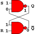
Below is the truth table for the low edge
triggered RS Flip-Flop
 actually change state, thisis
important. If R and S are held low (0) the states of the "Qs" remain
unaltered. As soon as a high
signal comes in, the state changes. This is called high or
positive logic. A functionally equivalent circuit could be
built that only reacted to the incoming of a low state (negative
logic).
 The only structural difference is that the circuit is built with NAND GATES, instead of NOR GATES...
| S |
R |
Q |
 |
| 0 |
0 |
0 - disallowed state | 0 - disallowed state |
| 0 |
1 |
1 |
0 |
| 1 |
0 |
0 |
1 |
| 1 |
1 |
Stays
the same |
Stays the same |
On this style of
RS Flip-Flop, S and R would normally be held HIGH, to maintain the
state. If S momentarily dropped low Q would go
high and  would go low. If R were to
momentarily drop low the opposite would happen. On the RS Flip-Flop
built with NOR gates, from the previous example, the change happened
from the change to high rather than the change to low.
To better illustrate this idea, consider the following example.
The button labeled "type 1" triggers an alert menu to popup when the mouse button goes down. The type 2 button triggers the event when the mouse button is released. Try it. This is similar to the difference between positive and negative triggered logic. This concept is important when interfacing different logic blocks. Lets say you have a device that outputs high when the temperature is above 100 degrees Celsius and another device that sounds a buzzer when the input goes low. With those specifications, the two devices would not be readily interfacable and an inverter would have to be used to bridge the two together.
 would go low. If R were to
momentarily drop low the opposite would happen. On the RS Flip-Flop
built with NOR gates, from the previous example, the change happened
from the change to high rather than the change to low.
would go low. If R were to
momentarily drop low the opposite would happen. On the RS Flip-Flop
built with NOR gates, from the previous example, the change happened
from the change to high rather than the change to low.To better illustrate this idea, consider the following example.
The button labeled "type 1" triggers an alert menu to popup when the mouse button goes down. The type 2 button triggers the event when the mouse button is released. Try it. This is similar to the difference between positive and negative triggered logic. This concept is important when interfacing different logic blocks. Lets say you have a device that outputs high when the temperature is above 100 degrees Celsius and another device that sounds a buzzer when the input goes low. With those specifications, the two devices would not be readily interfacable and an inverter would have to be used to bridge the two together.